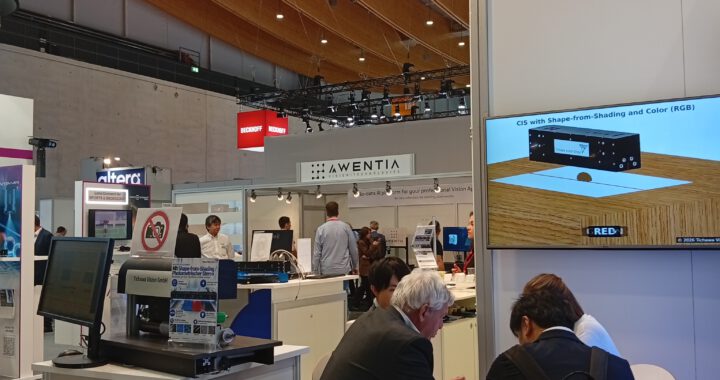
VISION 2026 in Stuttgart, held from October 6–8, provided an excellent opportunity to showcase the latest developments in industrial machine vision and discuss real-world inspection challenges with customers, partners, and industry experts.
We would like to sincerely thank everyone who visited us in Hall 10, Booth H20.
Our exhibition focused on Contact Image Sensor (CIS) technology for automated quality inspection. Two solutions attracted particular interest: WaferCIS, designed for high-resolution wafer inspection, and BergKristall with Shape-from-Shading technology, developed to detect extremely fine surface structures and defects.
The many valuable conversations at VISION 2026 once again demonstrated the diverse requirements of industrial machine vision and the potential of compact, application-specific CIS systems for inline quality inspection.
Our Highlights at VISION 2026
At VISION 2026 in Stuttgart, we presented our latest technologies and developments for industrial surface inspection.
Our key highlights included:
- WaferCIS: High-resolution wafer inspection with extended depth of field and versatile illumination options.
- BergKristall: High-speed, high-resolution surface inspection using Shape from Shading to detect even the smallest defects and height variations.
- Customized CIS solutions: Sensor configurations tailored to different materials, inspection requirements, resolutions, and scan widths.
- Compact inline integration: Seamless integration of image acquisition into existing production lines.
Beyond the technology demonstrations, we particularly appreciated the opportunity to exchange ideas about specific industrial applications and customer requirements.
WaferCIS: High-Resolution Wafer Inspection with Extended Depth of Field
With our WaferCIS, we demonstrated a compact solution for industrial wafer inspection, particularly suited to thin and back-thinned wafers.
One of the key challenges in wafer inspection is the reliable detection of fine defects, even when variations in surface height or object positioning occur.
Our WaferCIS addresses these challenges by combining high optical resolution, extended depth of field, and more than 25 illumination geometries.
By selecting the appropriate illumination configuration, different surface features and defect types can be made visible and captured for subsequent automated image processing.
The compact design of Contact Image Sensor technology also enables space-saving integration into industrial inspection equipment.
Learn more about our wafer inspection technology in our article on SEMICON Europa 2025.
BergKristall: Detecting the Finest Surface Defects with Shape from Shading
Another highlight of our exhibition was BergKristall with Shape-from-Shading technology.
The system combines high-resolution image acquisition with high inspection speeds and specialized illumination to reveal even the finest surface structures and height variations.
During our live demonstration, we used a rapidly rotating drum featuring a raised test pattern. This setup demonstrated how surface profiles and defects can be captured and analyzed while the object is moving.
A particular focus was the inspection of Braille lettering. The demonstration illustrated how the technology can reveal raised structures and support automated quality control.
Shape-from-Shading technology uses illumination from different directions to obtain information about surface topography.
This enables the detection and analysis of structures that may be difficult to identify using conventional two-dimensional imaging.
For further insights into this technology, read our article about high-speed 3D scanners for web inspection.
CIS Technology for Inline Quality Inspection
The live demonstrations at VISION 2026 highlighted the advantages of compact Contact Image Sensors in industrial machine vision.
In CIS systems, the sensor, optics, and illumination are positioned close to the inspection object. This compact architecture enables consistent image acquisition across wide scan widths and simplifies integration into existing production lines.
The technology offers particular advantages in applications where installation space is limited or high production speeds are required.
Depending on the inspection task, different sensor and illumination configurations can be used:
- RGB and monochrome image acquisition
- UV and IR illumination
- Shape from Shading for surface topography analysis
- Different resolutions, working distances, and scan widths
- Application-specific illumination geometries
These configuration options allow CIS systems to be tailored to individual production environments and inspection requirements.
Industrial Machine Vision Applications Across Different Industries
In addition to our live demonstrations, discussions about specific inspection challenges were a central part of our participation at VISION 2026.
We exchanged ideas with visitors from a wide range of industries, including:
- Semiconductor manufacturing: Inspection of wafers and sensitive surfaces
- Battery production: Inspection of electrode foils, separators, and bipolar plates
- Glass and display manufacturing: Detection of surface defects and structural irregularities
- Printing industry: Quality inspection of digital printing, decorative printing, and functional coatings
- Film and paper manufacturing: Inline inspection of continuous materials
- Metal processing: Inspection of sheet metal and precision surfaces
- Packaging industry: Inspection of surfaces, printed patterns, and embossed structures
- Printed electronics: Inspection of printed electronic structures and circuit boards
Optical inspection tasks involving coatings and material properties were also frequently discussed.
These conversations highlighted the importance of selecting the right sensor configuration based on material characteristics, defect size, production speed, and available installation space.
From Individual Inspection Challenges to Customized CIS Solutions
VISION 2026 once again confirmed an important principle: There is rarely a universal solution for industrial machine vision.
Every surface, material, and defect type presents unique requirements for sensor technology, optics, illumination, and image processing.
At Tichawa Vision, we therefore evaluate each inspection task individually.
Our application specialists examine original product samples under realistic conditions to determine which characteristics and defects can be detected automatically.
Based on these tests, we identify the most suitable combination of CIS technology, illumination, resolution, and scan width for the application.
Our goal is to develop a powerful, compact sensor system that adapts to your production environment – not the other way around.
Thank You for the Inspiring Conversations at VISION 2026!
We look back on a successful exhibition filled with valuable discussions, new ideas, and exciting industrial inspection challenges.
Thank you to everyone who visited us at VISION 2026 in Stuttgart.
We look forward to continuing these conversations and developing innovative machine vision solutions together.
Do You Have an Inspection Challenge?
Send us samples of your products!
Our application specialists will evaluate your original samples and work with you to identify a suitable CIS solution for your quality inspection requirements.
Contact us – we look forward to your challenge!