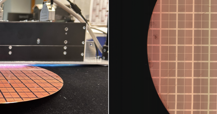
Special requirements for the inspection of wafers
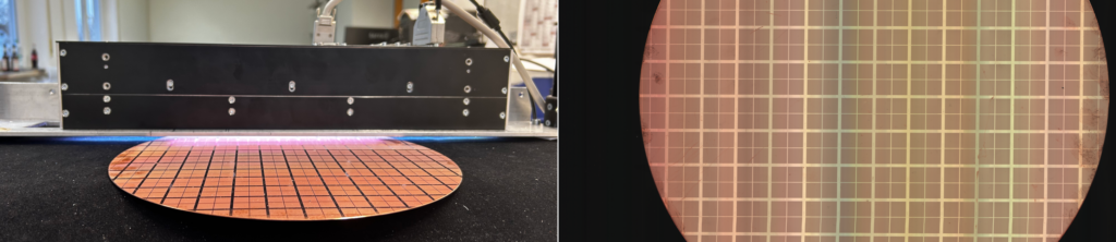
Optical wafer inspection plays an important role in semiconductor production in order to manufacture microchips with flawless quality. Optical systems are used to detect scratches, defects or particles on wafers.
The requirements placed on the camera system used for this are very demanding. A high resolution is required to see small defects in the micrometre range, special lighting, as the material is often very shiny, high processing speed and multiple calibration data for the various surface properties of the wafers. Often a lack of space is also a problem because the inspection system has to be installed in existing systems.
Tichawa Vision has developed a Contact Image Sensor especially for wafer inspection: The sensor has a resolution of 1200dpi, coaxial illumination, gapless image capturing at an overall installation height of only 110mm. The storage of multiple calibration data sets allows fast switching between different wafer types.